Measuring microflows Research on microflow sensors

Our main products include the so-called gas meters and tap water meters that are products for measuring the amounts of use of gases and tap water.
For instance, in ordinary homes, the amount of tap water flow per minute is about 12 liters if the amounts of tap water used for hand washing, cooking, bathing are averaged. Namely, the water meters installed in ordinary homes measure 12 liters/minute of water.
Therefore, water meters used in ordinary homes are designed to be able to measure the range of flow rate of about 0.5 liters/minute – 50 liters/minute.
As a flow meter manufacturer, we are aiming to improve our technologies while repeating trial and error by considering to what extent microflows can be measured, and which kinds of methods enable measurement.
Sensors for measuring microflows
In order to measure microflows, flow sensors need to be reduced in size. As an effective method for making such small sensors, we have focused on MEMS (Micro Electro Mechanical Systems). Among MEMS sensors in which mechanical structures are built on a silicon substrate or glass substrate by utilizing semiconductor manufacturing technologies, a lot of products are also commercialized as pressure sensors and acceleration sensors.
We have been taking approaches to realizing microflow sensors by means of MEMS technologies whereby silicon substrates are processed by semiconductor manufacturing technologies, and have successfully made a prototype that can measures the range of flow rates of 1μL/min. – 100μL/min.
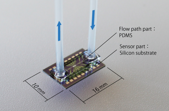
■ Overview of the microflow sensor
In the flow sensor that has been made as a prototype this time, the sensor part is formed with a silicon substrate, and the flow path part is formed with polydimethylsiloxane (PDMS), a type of silicone elastomer.
The sensor part is provided with functions as a heater and a resistance temperature detector, by forming a platinum thin film pattern on the top surface of the silicon substrate provided with a nitride film. Also, in order to reduce the thermal capacity of the sensor part, the silicon on the bottom surface of the platinum thin film pattern has been removed by means of an anisotropic etching. In the flow path part, PDMS is caused to flow into a mold that has been made beforehand, and after going through a hardening, the PDMS is cut out and pasted onto the aforesaid silicon substrate. And finally, the prototype has been completed by attaching a silicone tube.
The research and development have been done under the guidance provided by the Tabata Laboratory, Graduate School of Engineering, Kyoto University.
■ Measuring principles of the flow meter
The microflow sensor of which prototype has been made this time is a thermal wire type sensor whose sensing mode is such that the flow rate is sensed by using the platinum thin film pattern as a heater or a resistance temperature detector, and it has enabled measurements based on 3 basic principles:
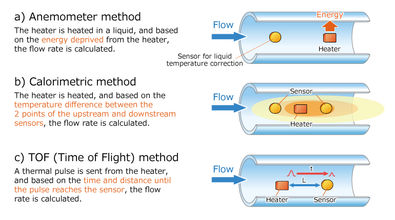
■ About the sensor output
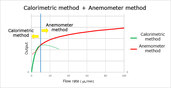
By combining the outputs of the anemometer method and calorimetric method that have been presented above in the basic principle of the thermal wire type, ideal flow rate measurements have been enabled. The calorimetric method has a narrow measurement range, but gives a greater change in relation to the flow rate, and whereby enables measurements with high accuracy. Also, it enables a distinction of the 0 point where there is no flow and of the forward or reverse direction. In the meantime, in the anemometer method, it is very difficult to distinguish the 0 point or the direction of flow, but the method is featured by the fact that the flow rate range of monotonic increase is wide. By obtaining an output by combining these measuring principles, the 0 flow rate and and the direction of flow can be distinguished, and thus we have successfully made a prototype of the microflow sensor measuring a wide flow rate range.
Toward commercialization
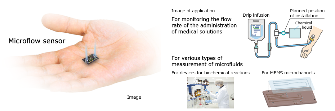
Toward commercialization, there are issues to be solved such as accuracy and durability, yield and others, but as the applications of microflow sensors, it is assumed that they will be used for the administration of pharmaceuticals and for built-in into analytical equipment, and the like. Also, we will continue the research and development of sensors that utilize MEMS technologies besides the flow sensors as well, so that we will be able to bind the R&D with improvements in technologies and commercialization needs.
Voice of a developer

■ What was a big issue in the research and development of the microflow sensor?
We had difficulties in finding a way to electrically insulate the sensing part that has been formed with a platinum thin film pattern, in order to measure the flow rate of liquids having electrical conductivity. At first, as we had learned that a film devoid of defects such as pinholes can be formed in complex structures, we formed an insulation film by using an organic film. Although we made improvements while gathering information, the film was inadequate in terms of durability as an insulation film for thermal flow sensors. Meanwhile, insulation films made of silicon oxide films and nitride films had problems in that their electrical insulation performance was inadequate due to defects such as pinholes, rather than their durability. However, we have found in the process of trial and error that the coverage of defects by the accumulation of layers is effective, and we have successfully improved electrical insulation performance by using a multi-layered film of silicon oxide films and nitride films as the electrical insulation film.
Relevant information
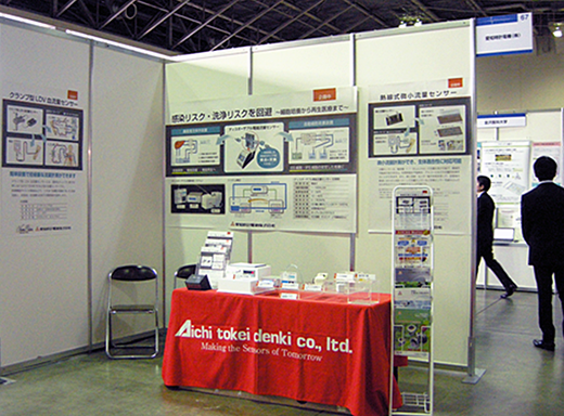
Concerning the microflow sensors presented here, we exhibited the prototype and distributed handouts in exhibitions and academic meetings, etc.
It was exhibited in the 4th Medical Messe Nagoya and in the 5th Joint Conference of the Research Center for Advanced Biomechanics. &. Japan Institute of Electronics Packaging Kyushu Branch.